Technology
Specialty Fab in Japan: TSMC to Build It To Address Local Demand
As confirmed by Taiwan Manufacturing Semiconductor Co., TSMC will build its first semiconductor manufacturing facility in Japan. As expected, the operations will start in 2023 or 2024 for specialty fab in Japan.
Specialty Fab in Japan: All About Its Development
Mature and specialty process technologies will be used to produce the specialty chips by the fab. These specialty chips will enhance the supply of components the local clients that include automakers as well. It means that its fabs outside of Japan will make it possible to allocate more capacity for various PC applications.
What does the chief executive officer of TSMC say about specialty fab in Japan?
The chief executive officer of TSMC, CC Wei, said at the conference call with financial analysts and investors that after making careful examination and inspections, he and the company announced their intention to build a specialty technology fab in Japan. Furthermore, its approval is dependent on their board of directors. Moreover, it was also declared that both their customers and the Japanese government strongly commit to supporting this project.
What will the TSMC’s semiconductor production facility in Japan process?
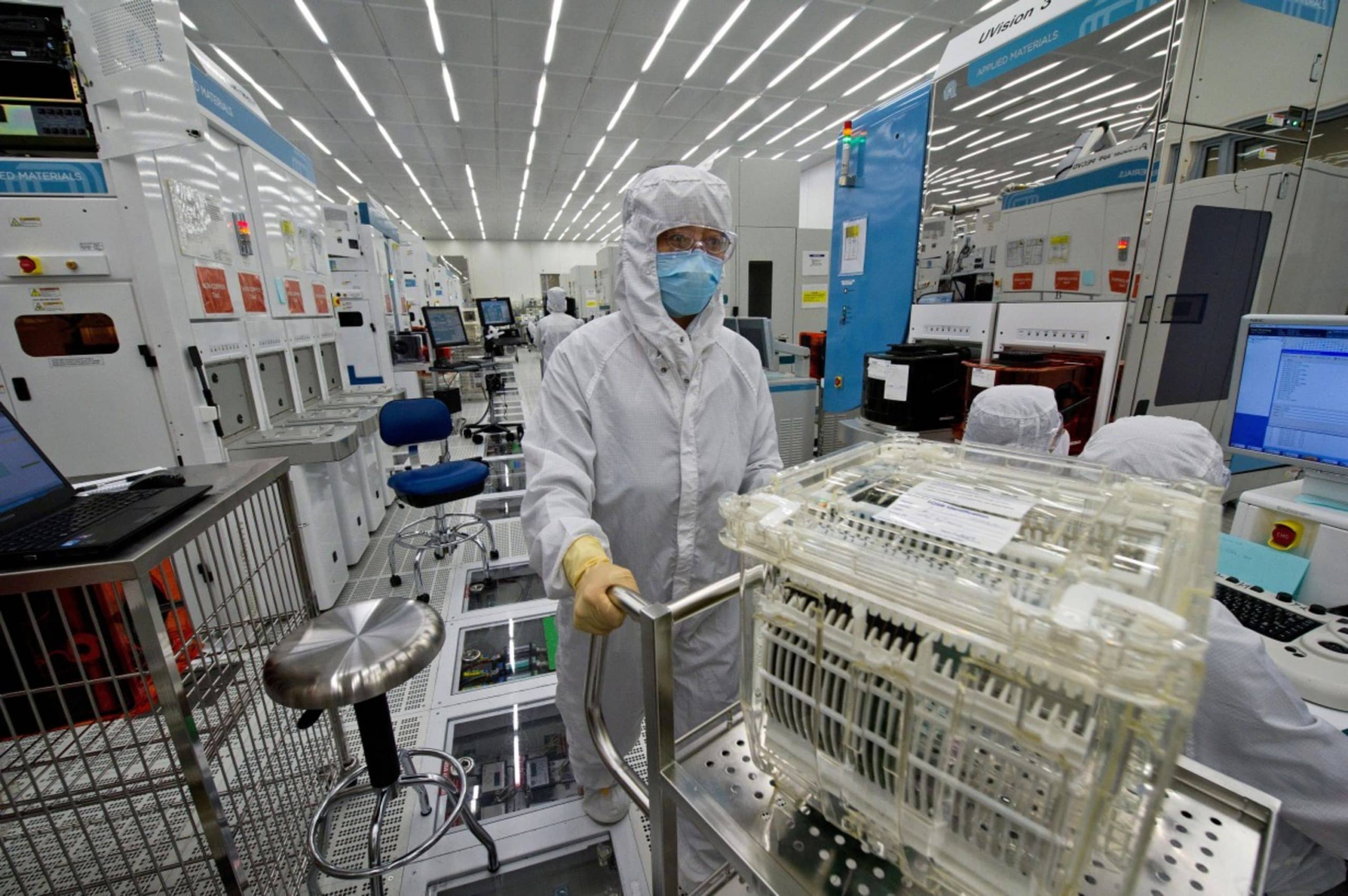
Using several 28 nm-derived fabrication processes, specialty fab in Japan, will process wafers. These fabrication processes include a great many 28 nm nodes and 22ULP nodes as well for ultra-low-power applications. Though these manufacturing technologies are traditionally old-fashion for applications such as high-performance CPUs or GPUs and smartphone system-on-chips, they are quite good for chips that the automotive and consumer electronics industries use. Moreover, since many ICs have a long lifecycle, these manufacturing technologies will be sufficient for years to come.
Beginning of the construction of specialty fab in Japan
The construction of the fab will start in 2022 by TSMC. In the late 2024, TSMC expects it to start the operations. Adding to his statement about the specialty fab, Wei also said that 20 nm to 28 nm technology will be utilized by the fab for semiconductor wafer fabrication. Moreover, he also said that fab construction will begin in 2022 and the production will start in the late 2024.
Why they are building it?
TSMC is the world’s largest foundry and because of geopolitical situation as well as surging demands for chips it is expanding beyond Taiwan. Rumours have it that for months that they have intentions to build specialty fab in Japan. But after making careful inspections, the company confirmed the specialty fab production in July. In the past few months, the company assessed the needs of its clients in Japan, built up operating efficiency and costs, and hence, it concluded that building fab in Japan makes sense.
The company already collaborates with the University of Tokyo in several areas, and it’s building an R&D centre in Japan as well. Since the company’s local ties are good, it’s reasonable for the company to expand its presence in Japan with a manufacturing facility.
What’s the cost of specialty fab in Japan?
The company hasn’t disclosed the cost of fab or planned capacity for it yet. Moreover, the company neither confirmed nor denied any involvement of the Japanese government and Sony in the project. According to reports by Nikkei that the estimated cost of the production is about $7 billion. According to the agency, authorities will be investing half of the fab cost. On the other hand, Sony would take a minority stake. According to Nikkei, the location of the production facility will be on thee electronics giant’s land near Sony’s image sensor fab in Kumamoto Prefecture.

Vampire Crawlers Coin Farming Guide

Forza Horizon 6 Performance: Why 60 FPS Is Still the Console Standard

Yoshi and the Mysterious Book (2026) – Full Completion Guide, Rewards & Secret Ending

How to Get Free Pets in Adopt Me: A Guide for Players

Roblox Username Generator – Create a Cool & Unique Username in Seconds
How to Get Free Pets in Adopt Me: A Guide for Players
Yoshi and the Mysterious Book (2026) – Full Completion Guide, Rewards & Secret Ending
Vampire Crawlers Coin Farming Guide