News
With their ’12nm-class’ RAM, Samsung claims to bring DDR5 to the market
Samsung has revealed a new generation of its DDR5 random access memory (opens in new tab), which the company claims is the first “12nm class” memory in the world. According to Samsung, the compatibility evaluation with AMD Ryzen 7000 Series platforms (opens in new tab) has already been finished, which means that the chips are ready to be installed into AM5 motherboards.
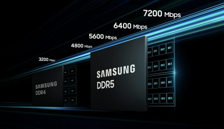
This new 12nm-class DRAM is believed to be capable of speeds of up to 7.2Gbps, which translates to 60GB/s of bandwidth when applied over an entire system. In addition to this, Samsung asserts that the new memory chips can compete for the title of having the best data density in the industry.
“This technological advance was made possible by the introduction of a novel high-K material that boosts cell capacitance as well as proprietary design technology that improves critical circuit characteristics. Both of these factors contributed to the overall improvement of critical circuit characteristics. The new DRAM has the highest die density in the industry, which enables a 20 percent increase in wafer productivity. This is made possible by the combination of cutting-edge, multi-layer extreme ultraviolet (EUV) lithography and the new DRAM “Samsung’s announcement says (opens in new tab).
Additionally, power consumption is reduced by 23% in comparison to Samsung’s already cutting-edge DDR5 technology. The capacity of each chip in the brand-new DDR5 is still 16 gigabytes. Naturally, it is important to take note of the most important qualifier in all of this, which is the use of the word “class.” The phrase “12nm” does not truly translate to the physical size of elements within memory chips, just as it does not correspond to the process technology that Intel and TSMC employ for central processing units (CPUs) and graphics processing units (GPUs). When referring to where the new memory fits in Samsung’s product stack, the term “relative” is more accurate.
Other memory manufacturers, such as SK Hynix and Micron, for instance, assert that they have created 10nm-class DDR5 chips in their products. However, Samsung claims that this new DDR5 has the highest density of any previous version. Marketing figures, eh?
In any case, what we can do is keep our fingers crossed that the “12nm” technology will result in additional price reductions for DDR5 due to the new density. The chips ought to be made at a smaller scale and at a reduced cost. According to Samsung, “our 12nm-range DRAM will be a significant enabler in pushing market-wide adoption of DDR5 DRAM.” This statement was made to support the aforementioned point.
When exactly this market-wide acceptance will take place is not something that can be said to be absolutely imminent. It is anticipated that mass manufacturing will start in 2023, which means that it will be at least three months before we see memory DIMMs equipped with the new chips.
Since Intel’s Alder Lake became the first CPU to adopt the new standard before the end of 2017, costs for DDR5 memory have experienced a significant drop. However, costs are still close to being twice as high as those of DDR4. So here’s hoping that this new 12nm Samsung kit keeps those prices falling, regardless of how large the bits truly are that are contained within it.

Vampire Crawlers Coin Farming Guide

Forza Horizon 6 Performance: Why 60 FPS Is Still the Console Standard

Yoshi and the Mysterious Book (2026) – Full Completion Guide, Rewards & Secret Ending

How to Get Free Pets in Adopt Me: A Guide for Players

Roblox Username Generator – Create a Cool & Unique Username in Seconds
How to Get Free Pets in Adopt Me: A Guide for Players

Grow a Garden Recipes in Roblox: Guide to Cook (Donuts, Sushi, Pie, Pizza & More!)
Roblox Username Generator – Create a Cool & Unique Username in Seconds
Yoshi and the Mysterious Book (2026) – Full Completion Guide, Rewards & Secret Ending